

News
“Smart skin” can identify weaknesses in bridges and airplanes using laser scanner
Recent research results have demonstrated that two-dimensional, on-demand mapping of the accumulated strain on metal structures will soon be a reality thanks to an engineered “smart skin” that’s only a fraction of the width of a human hair. By utilizing the unique properties of single-walled carbon nanotubes, a two-layer film airbrushed onto surfaces of bridges, pipelines, and airplanes, among others, can be scanned to reveal weaknesses in near real-time. As a bonus, the technology is barely visible even on a transparent surface, making it that much more flexible as an application.
Stress-inducing events, along with regular wear and tear, can deform structures and machines, affecting their safety and operability. Mechanical strain on structural surfaces provides information on the condition of the materials such as damage location and severity. Existing conventional sensors are only able to measure strain in one point along one axis, but with the smart skin technology, strain detection in any direction or location will be possible.
How “Smart Skin” Technology is Used
In 2002, researchers discovered that single-wall carbon nanotubes fluoresce, i.e., glow brightly when stimulated by a light source. Later, the fluorescence was further found to change color when stretched. This optical property was then considered in the context of metal structures that are subject to strain, specifically to apply the property as a diagnostic tool. To obtain the fluorescent data, researchers applied the smart skin to a testing surface, irradiated the area with a small laser scanner, and captured the resulting nanotube color emissions with an infrared spectrometer. Finally, two-dimensional maps of the accumulated strain were generated with the results.

The primary researchers, Professors Satish Nagarajaiah and Bruce Weisman of Rice University in Texas, have published two scientific papers explaining the methods used for achieving this technology and the results of its proof-of-principle application. As described in the papers, aluminum bars with holes or notches in areas of potential stress were tested with the laser technique to demonstrate the full potential of their invention. The points measured were located 1 millimeter apart, but the researchers stated that the points could be located 20 times closer for even more accurate readings. Standard strain sensors have points located several millimeters apart.
What Are Carbon Nanotubes?
Carbon nanotubes (CNTs) are carbon molecules that have been structurally modified into cylinders, or rather, rolled up sheets of carbon atoms. There has been some evidence suggesting that CNTs can be formed via natural processes such as volcanic events. However, to really capitalize on their unique characteristics, production in a laboratory environment is much more efficient.
Several methods can be used for production, but the most widely used method for synthesizing CNTs is chemical vapor deposition (CVD). This process combines a catalyzing metal with a carbon-containing gas which are heated to approximately 1400 degrees Fahrenheit, triggering the carbon molecules to assemble and grow into nanotubes. The resulting formation resembles a forest or lawn grass, each trunk or blade averaging .43 nanometers in diameter. The length is dependent on variables such as the amount of time spent in the high heat environment.

Besides surface analysis, carbon nanotubes have proven invaluable in many research and commercial arenas, their luminescence being only one of many properties that can improve and enable other technologies. Their mechanical tensile strength is 400 times that of steel while only having one sixth the density, making them very lightweight. CNTs also have highly conductive electrical and thermal properties, are extremely resistant to corrosion, and can be filled with other nanomaterials. All of these advantages open up their applications to include solar cells, sensors, drug delivery, electronic devices and shielding, lithium-ion batteries, body armor, and perhaps even a space elevator, assuming significant advances overcome its hurdles.
Next Steps
The nanotube-laced smart skin is ready for scaling up into real-world applications, but its chosen industry may take time to adopt given the general resistance to change in a field with long-standing existing technology. While awaiting embrace in the arena it was primarily designed for, the smart skin has other potential uses in engineering research applications. Bruce Weisman, also the discoverer of CNT fluorescence, anticipates its advantages being used for testing the design of small-scaled structures and engines prior to deployment. Niche applications like these may be the primary entry point into the market for some time to come. In the meantime, the researchers plan to continue developing their strain reader to capture simultaneous readings from large surfaces.
 -
-

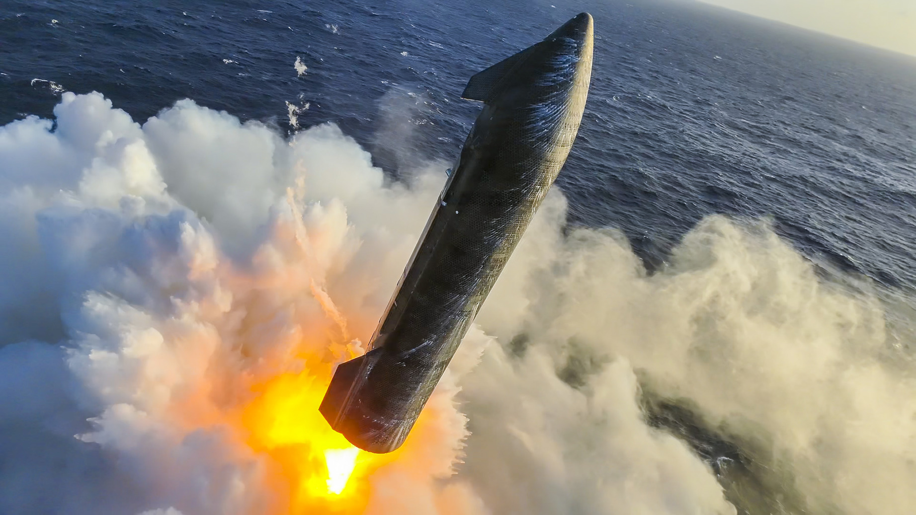
Elon Musk shed two new bits of detail on Starship following its 13th test launch, which was an overwhelming success.
SpaceX launched Starship for the 13th time last Friday after two delays: one on Monday when several Raptor engines did not ignite, and another on Thursday due to unfavorable weather conditions in Starbase, Texas.
The launch was overwhelmingly successful. SpaceX was able to complete a necessary test of the heat shield tiles by increasing the acceleration of Starship from launch throughout the flight; 20 Starlink v3 satellites were released with no issue; the Super Heavy Booster landed safely in the Gulf of America, Ship successfully reignited engines while in space; and it also splashed down without incident in the Indian Ocean.
SpaceX Starship just nailed something it’s never done before
Nevertheless, more details are coming out about Starship, and Musk is doing the talking.
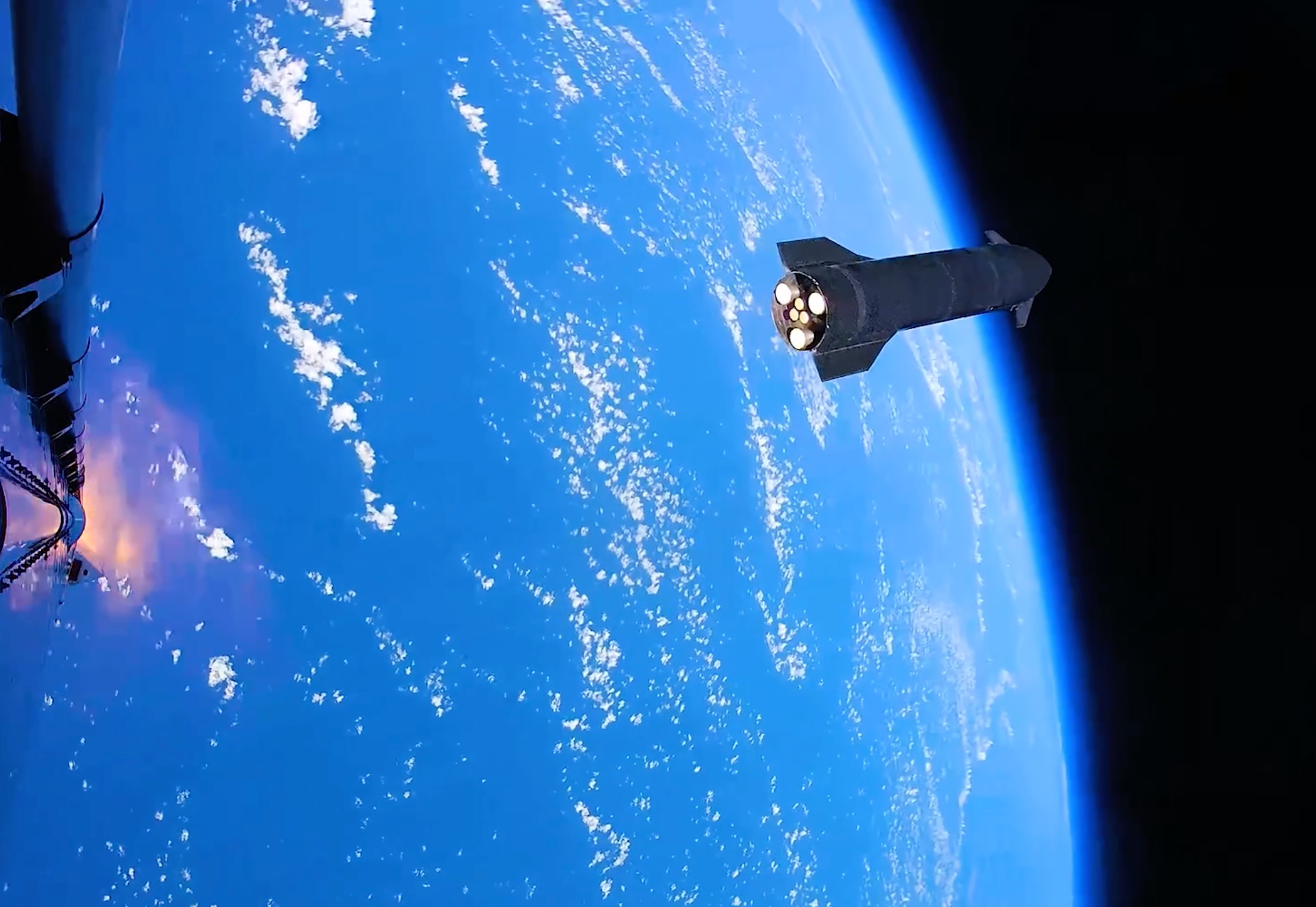
Starship Will Be Retrieved in the Ocean
Musk revealed on Tuesday night that Starship would be recovered by a ship in the Indian Ocean. SpaceX routinely tries to recover Starship after splashdown in an effort to find out more about the flight by examining the spacecraft afterward.
We’re sending a ship out to recover Starship https://t.co/fUqUZTITO9
— Elon Musk (@elonmusk) July 28, 2026
-
This helps engineers find out more about why things might have happened, allows them to examine any potential damage or anomalies that might have occurred, and increases the chances of an even more successful flight next time thanks to the additional information recovered.
Ship Could Have Been Caught by Tower Arms, Musk claims
Musk has already indicated that SpaceX will plan to attempt a catch of Starship with the 14th test flight. While this would be a major accomplishment, it would be an expected next step, considering the fact that the Super Heavy Booster has already been caught by the chopsticks on numerous occasions.
The ship landing was precise, meaning that it would have been caught by the tower arms https://t.co/6nbNrRfX9P
— Elon Musk (@elonmusk) July 29, 2026
A ship catch would be a great indication of where SpaceX stands in terms of reusability and launch cadence. A successful catch with relatively no incidents would be a good sign that SpaceX is nearing a more frequent launch of Starship, but also that the reusability of the massive rocket would be something many would expect in the near future.
It is a necessity to make life multiplanetary.
-

Elon Musk has updated his timeline for when humans will walk on Mars and for when ships will simply get there.
The objective of getting to Mars has been one of Musk’s biggest goals since becoming a serial entrepreneur and realizing that time on Earth is limited. Musk has said several times he hopes to die on Mars, and not by impact.
Musk now believes that people will be on Mars in “roughly 5 to 7 years.” He said that a Mars lander will get there “a few years sooner.”
People on Mars in roughly 5 to 7 years.
Mars lander a few years sooner.
— Elon Musk (@elonmusk) July 29, 2026
The response from Musk comes after NASA Administrator Jared Isaacman said that SpaceX’s biggest priority is the Moon and not Mars. Because of this, Isaacman conceded that he believes nuclear power and propulsion investments will provide “potentially the pathway with the fewest miracles required to put four people on Mars in the next 10 to 15 years.”
-
Of course, this is what NASA can do through taxpayer funding and nuclear investments, he added.
Musk’s grand ambitions are much more optimistic than most, and it is certainly a double-edged sword. This is not the first time timelines for Mars have been somewhat lofty, especially to those normal thinkers like you and me, not super geniuses like Musk.
In fact, the SpaceX and Tesla frontman has said on at least a dozen occasions that we could be on Mars in the coming years. Musk said 2020 would be the big year as early as 2009. In 2020, he was “highly confident” of a landing in 2026, and had even said 2024 in a best-case scenario.
The point is, the range has varied, and it’s anyone’s guess when we’ll get there. This latest adjustment to the timeline is typical of Musk, and while the Moon has seemingly taken priority over Mars, it is still worth mentioning that the ultimate goal is to make life multiplanetary, and it starts potentially with the Red Planet.
SpaceX (NASDAQ: SPCX) got an absolutely crazy price target rating from Raymond James after the company experienced a tough first few weeks following its Initial Public Offering (IPO).
Despite the tumultuous start, SpaceX has plenty of believers, and the company’s massively successful Starship launch last Friday, its 13th test flight of the massive rocket, went so smoothly that Raymond James analysts pushed its price target on the company to roughly 7 times its current trading level.
SpaceX Starship just nailed something it’s never done before
The firm officially put a “Strong Buy” rating and an $800 price target on the stock. It currently trades at around $113. Its all-time high is $225.64, reaching this trading level shortly after shares first went public.
Raymond James’ price target is tied to the firm’s confidence after Starship’s 13th test flight. Analysts at the firm said it was an incremental step that reduces engineering risks, citing the widely successful heat shield test that CEO Elon Musk recently detailed, the smooth deployment of Starlink V3 satellites, and a successful in-space engine relight.
SpaceX also managed to see Starship splash down safely in the Indian Ocean, while the Super Heavy Booster fell down to the Gulf of America with no incidents.
It is interesting to see these launches have such a tremendous impact on the stock and what investors think of it. After SpaceX initially delayed the Starship launch last week, shares fell tremendously. Most probably did not realize that the stand-down is a standard practice, especially if everything is not perfect.
-
The mission was initially aborted due to an issue with Raptor engines. This was resolved, and Starship launched last Friday after another delay on Thursday, which was caused by weather.
Now that analysts have seen what SpaceX launches are capable of and how impressive the feat is, firms are adjusting their price targets accordingly, making it known that they have high expectations for the space exploration company.

Elon Musk sheds two new bits of detail on Starship after 13th test launch

Elon Musk updates the SpaceX timeline for Mars


